Custom Board Level Shielding

Achieve perfect PCB fit and superior signal integrity with our strict tolerance fabrication. We offer DFM support, varied alloy options (Nickel Silver, Cold Rolled Steel, etc.), and prototyping in as little as 3 days.

What is Board Level Shielding (BLS)?

At its core, Board Level Shielding (BLS) is a stamped or etched metal enclosure designed to isolate sensitive components on a Printed Circuit Board (PCB). It acts as a conductive barrier, preventing internal signals from leaking out (EMI) and blocking external noise (RFI) from disrupting critical circuits.

For modern electronics, a generic metal can is rarely enough. At ShincoFab, we treat shielding as a precision component, not just a cover. We ensure your shield is manufactured as an integral part of your PCB design strategy for maximum regulatory compliance and long-term reliability.

Why Choose Custom Board Level Shielding?

Don’t compromise your board layout to fit a standard catalog part. ShincoFab’s custom shielding allows you to prioritize performance, ensuring optimal signal integrity without sacrificing valuable PCB real estate.
01.

Tailored to Your PCB Design

Off-the-shelf shields force you to design around them. We design for you.

  • Maximize Real Estate: Our custom designs utilize every available millimeter, fitting irregular shapes and tight corners to cover only specific interference zones, freeing up space for other critical components.
  • Perfect Fit: We adjust shield height and wall thickness to clear tall components while maintaining a low profile, ensuring seamless integration into slim device enclosures.
Board Level Shielding-1
02.

Advanced Manufacturing for Precision & Performance

Different production stages require different methods. We utilize a hybrid approach to guarantee precision:

  • Photo Chemical Etching: Ideal for intricate designs and prototypes. This stress-free process produces burr-free parts with no molecular deformation, crucial for high-frequency RF applications.
  • Precision Stamping: For high-volume production, our progressive die stamping ensures consistent repeatability and cost-efficiency.
  • Surface Treatment: We offer selective plating (Tin, Nickel, Gold) to enhance solderability and corrosion resistance according to your conductivity requirements.
03.

Enhanced Thermal Management

A shield shouldn’t be a heat trap. We treat thermal management as a key design parameter, not an afterthought.

  • Strategic Venting: We can incorporate custom perforation patterns or holes directly above hot components (like CPUs or PMICs) to facilitate airflow without leaking EMI.
  • Heat Sink Integration: Our engineers can design shields that double as heat sinks or include contact surfaces for thermal pads, solving two problems with one component.
Board Level Shielding-2
chinese engineer
04.

Expert Engineering Support

We are more than a machine shop. We are your DFM partners.

  • Design Consultation: Send us your Gerber files or STEP models. We actively review them to identify potential manufacturing bottlenecks that could drive up costs or cause assembly failures.
  • 3D Modeling & Validation: We verify co-planarity and flatness specs before production to ensure our shields work perfectly with your SMT pick-and-place equipment.
05.

Fast Turnaround & Scalable Production

Speed to market is critical. Our process is built to scale with your product lifecycle.

  • Rapid Prototyping: Utilizing soft tooling and laser cutting, we can deliver functional samples in as little as 3–5 days for validation.
  • Cost-Effective Scaling: As your demand grows, we transition seamlessly from low-cost prototyping tools to durable hard tooling, drastically reducing the per-unit cost for mass production.
Board Level Shielding Prototype

Select the Right Shielding Architecture for Your Application

Your choice of shielding configuration impacts not just EMI performance, but also assembly costs and future repairability. We manufacture a full range of configurations to match your specific maintenance strategies and board density requirements.

One-Piece Board Level Shields

One-Piece Board Level Shields

Best for high-reliability devices where post-assembly component access is not required.

  • Cost-Efficient: A single stamped unit implies lower tooling and unit costs compared to two-piece designs.
  • Robust Protection: Provides a continuous, gap-free enclosure for maximum shielding effectiveness.
  • Deep Drawn or Folded: Available in seamless deep-drawn options for high-frequency applications or folded designs for standard use.
Two-Piece Shields with Removable Lids

Two-Piece Shields with Removable Lids

Best for complex boards requiring inspection, tuning, or rework after assembly.

  • Damage-Free Access: Consists of a fence (frame) soldered to the PCB and a snap-on cover. Technicians can remove the cover to inspect components without desoldering the frame, eliminating the risk of thermal damage to the board.
  • Shock & Vibration Resistant: Our proprietary dimple-lock designs ensure the cover stays secure performing even in harsh environments like automotive or aerospace.

Multi-Compartment / Labyrinth Shields

Best for densely packed PCBs with multiple noisy circuits (e.g., separating RF transmitting from Power management).

  • Reduced BOM Count: Replaces multiple individual shields with a single, complex unit.
  • Cross-Talk Elimination: Internal walls/fences isolate different functional blocks within the same footprint, saving significant board real estate.
Thermal Management Shields

Thermal Management Shields (The Hybrid Solution)

Best for high-power chipsets that generate significant heat (CPUs, PMICs, GPUs).

  • Airflow Optimized: Features custom perforation patterns or honeycomb vents to allow heat escape without leaking EMI.
  • Heat Sink Ready: Designs can feature lower-profile tops or cutouts to allow direct contact between the component and a heatsink or chassis.

Select the Right Material for Your Environment

Achieving optimal shielding effectiveness (dB attenuation) starts with selecting the right alloy and ends with maintaining strict mechanical tolerances. We guide you through the material selection process to balance conductivity, galvanic compatibility, and cost.

Select the Right Material for Your Environment

We stock a wide range of standard and specialty metals. We recommend materials based on your specific designated frequency usage and environmental conditions.

  • Nickel Silver (Industry Standard): The preferred choice for most Board Level Shielding. It offers excellent solderability without post-plating, high permeability, and excellent corrosion resistance.
  • Cold Rolled Steel (CRS) / Mild Steel: A cost-effective option for high-volume production. Requires tin plating for solderability and corrosion protection.
  • Stainless Steel: Offers high strength and rigidity. Ideal for thin-gauge lids where dent resistance is critical. (Typically requires tin plating for soldering).
  • Copper Alloys (Beryllium Copper / Brass): Best for applications requiring maximum conductivity and attenuation. BeCu provides superior spring properties for two-piece shield clips.
  • Aluminum: Lightweight options for weight-sensitive aerospace or mobile applications (often requires conversion coating).

Manufacturing Methods Engineered for Scale

Whether you need 10 prototypes or 10 million units, we use the process that fits your volume and precision needs.

  • Photo Chemical Etching (PCE):
    Best for prototyping & complex geometries. A subtractive process that dissolves metal chemically. Guaranteed burr-free edges and no mechanical stress, ensuring the metal remains perfectly flat. No expensive hard tooling required.
  • Precision Stamping:
    Best for high-volume Production. Utilizing high-speed progressive dies to produce parts at the lowest possible unit cost with consistent repeatability.
  • Thermoforming / Forming:
    Used for specific 3D geometries or creating plastic-based shields with conductive coatings, offering lightweight alternatives to solid metal.

Plating & Surface Treatments

We offer both pre-plated materials and post-plating services to ensure conductivity and durability.

  • Tin Plating: For optimal solderability (Bright or Matte finish).
  • Nickel: For wear resistance and corrosion protection.
  • Gold / Silver: For low contact resistance in high-performance contact areas.
Board Level Shielding

Coplanarity Assurance for SMT Assembly

The failure of a shield often happens at the assembly line, not in the field.

  • Strict Flatness Tolerances: We understand SMT. Our shields are manufactured with strict coplanarity (typically within 0.08mm – 0.10mm) to ensure 100% reliable solder joints during reflow.
  • Tape & Reel Packaging: All SMD parts can be packaged in EIA-481 compliant carrier tape for seamless pick-and-place automation.

Extend Your R&D Capabilities with Expert Engineering Support

Designing effective EMI shielding often comes late in the board layout process, leading to space constraints and thermal challenges. We take that burden off your shoulders. Our engineering team bridges the gap between your digital CAD file and a physical, functional component.

Comprehensive Design Consultation (DFM)

Don’t wait until production to find out a part won’t fold correctly.

  • DFM Reviews: We conduct thorough Design for Manufacturability (DFM) reviews on every project. We identify potential weak points—such as bend radii that are too tight or walls that are too thin—and propose minor adjustments that significantly reduce manufacturing costs and failure rates.
  • Thermal & EMI Optimization: Struggling with heat dissipation? We can advise on the optimal placement of ventilation holes or thermal pad contact points without compromising EMI attenuation.
chinese engineer DFM
Board Level Shielding Design

Flexible Engineering for New Designs and Legacy Parts

  • New Designs: Starting from a blank slate? Give us your PCB layout (Gerber/DXF), and we will design a shield model that fits your component heights and keep-out zones perfectly
  • Legacy Part Replacement: Need to replace a discontinued clip or upgrade an old shield design? We can reverse-engineer existing parts or update legacy drawings to modern manufacturing standards.

Rapid Prototyping to Test Before You Invest

Speed is the currency of modern electronics. We help you validate your design without the financial risk of hard tooling.

  • Soft Tooling Solutions: Using laser cutting and photo-etching, we can produce engineering samples in as little as 3–5 days.
  • No/Low Tooling Costs: Avoid the commitment of expensive progressive dies during the testing phase. Iterate your design freely and affordable until it’s perfect, then scale up seamlessly.
Board Level Shielding Prototype-1

Trusted Custom Board Level Shielding for Critical Industries

From rigorous ADAS safety standards to critical medical device compliance, our shielding solutions deliver zero-defect performance where reliability is non-negotiable.

Frequently Asked Questions

Everything you need to know about our fabrication process. Clear details on lead times, material selection, and how we transition you from prototyping to high-volume production.

What coplanarity tolerances can you hold for SMT shields?

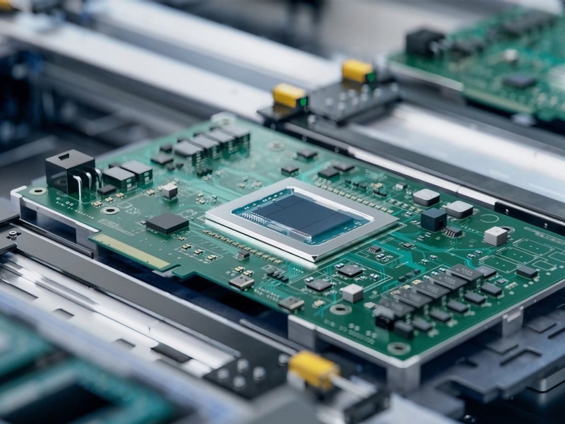
This is critical for SMT reflow. We typically maintain a coplanarity flatness of 0.08mm to 0.10mm (depending on size) to ensure 100% reliable solder joints. We perform automated optical inspection to verify flatness before packaging.

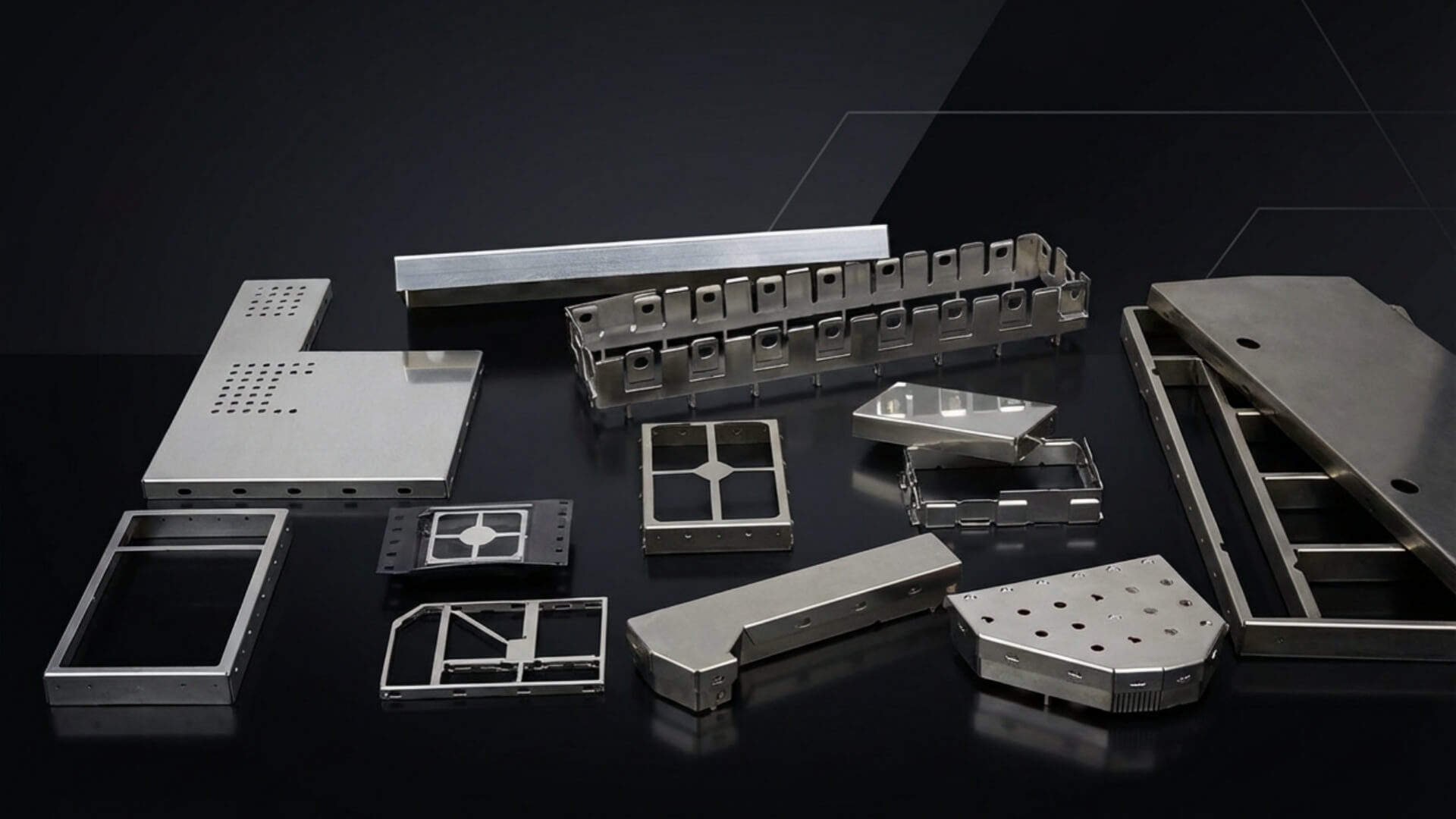
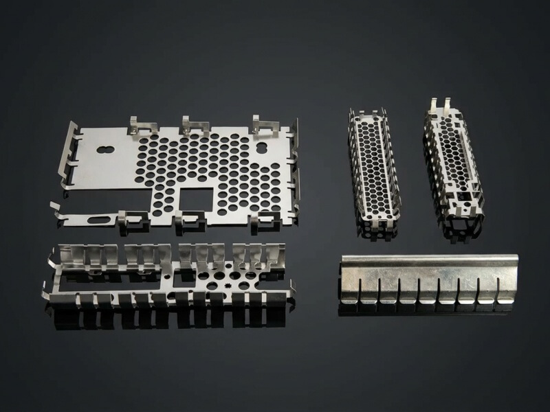
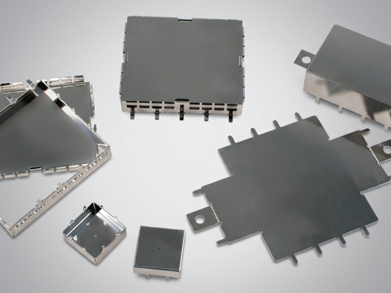
Yes. For high-frequency applications where corner leakage is a concern, we produce deep drawn shields that are naturally seamless. We can also weld or solder the corners of standard folded shields to ensure a continuous RF seal.

We don’t just ship in bags. For volume production, we deliver SMT shields in EIA-481 compliant Tape & Reel packaging, ready for immediate loading onto your pick-and-place machines. Trays are also available for larger or odd-shaped parts.

We can work with STEP / STP 3D models, DXF / DWG 2D drawings, or even Gerber files from your PCB layout. If you only have a rough sketch, our engineering team can help convert it into a manufacturable CAD model.

Custom production does not mean high upfront costs. We scale the manufacturing method to match your budget and stage of development.

  • For Prototypes: We use Photo Etching or Laser Cutting. These methods require zero or minimal tooling investment, allowing you to test designs without financial risk.
  • For High Volume: We transition to progressive die stamping. While this involves hard tooling, it drastically lowers your per-unit price. You only invest in the tool when your production volume justifies the savings.
  • Prototypes: Typically 3–5 business days using soft tooling methods.
  • Mass Production: Typically 2–3 weeks after tooling approval. We also offer expedited services for urgent NPI (New Product Introduction) deadlines.

Nickel Silver is our top recommendation for most applications because it is solderable without post-plating and highly corrosion-resistant. We also work with Cold Rolled Steel (CRS) (needs Tin plating), Stainless Steel, and Beryllium Copper for specific spring-contact requirements.

Yes. We can design shields with custom perforation patterns to maximize airflow, or create open-top frames that allow a heat sink to directly contact the component. We can also pre-apply thermal interface materials inside the shield if required.

Get a Free DFM Review & Quote Within 24 Hours

Upload your STEP, DXF, or Gerber files securely. Our engineering team will review your design for manufacturability, suggest potential cost-savings, and return a comprehensive quote.

Whatsapp

+86 13392819510

Address

Building 1, No.8, Second Street, Huangjiang Town,
Dongguan City, Guangdong Province

Socials

Please enable JavaScript in your browser to complete this form.
Click or drag files to this area to upload. You can upload up to 3 files.
Scroll to Top

Let's Talk About Your Project